 |
| |

|
|
Applications
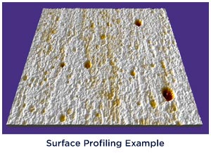 Surface profiling and features measurement Surface profiling and features measurement
Using AEP profilers — contact and/or optical based techniques AEP metrology can virtually do Surface profiling such as defect measurement, surface feature analysis etc.for any type of surface.
Following are recommendations for choice of technique
Optical Profilometer NanoMap-O
- Both below mentioned modes present on
same head as a part of basic package.
- Scanning white light /coarse mode for
150nm< Surface profile <10mm.
- Phase shift/fine mode—Surface profile < 150nm.
For product information click here.

Contact Profilometer NanoMap-LS
- Measures Surface profile up to 500 microns (0.5mm) with high spatial resolutions.
- More effective than optical profilometer on samples with larger slopes or on material with unknown optical constants. Its also more effective on dirty samples.
For product information click here.
Contact + Optical Profilometer NanoMap-D
- Model NanoMap has both Contact and Optical profilometer on same platform. It can be used to measure Surface profile of ANY kind sample—thin , thick, dirty, non flat etc. Range nm to 10mm.
For product information click here.
|
| |
 |
|
|
